Gallium nitride (GaN) and SiC semiconductor devices have already been around for some years. The first one proliferated due to the necessity of high frequency operation in optoelectronics applications. On the other hand, Schottky SiC power diodes were introduced in 2001 as an alternative to eliminate reverse recovery issues in Si rectifiers.
Wide band-gap semiconductors offer increased electrical field strength and electron mobility compared to Si semiconductors. Moreover, both semiconductor materials are particularly interesting for high temperature operation. These characteristics make integration of SiC and GaN devices as the next logical step to further increase efficiency and power density in SMPS.
First, an overview of current state-of-the-art semiconductor technology in the 600/650 V range, and recent developments on the integration of GaN devices in SMPS are provided. The second part of the thesis provides an insight on semiconductor characterization and compares state-of-the-art Si technology to current available GaN switches. After this overview, a comparison between continuous (CCM) and boundary conduction modes (BCM) in PFC applications is provided based on the semiconductor characterization data.
The comparison takes into consideration the electromagnetic interference (EMI) filter size and the converter input inductor volume, as a necessary part for evaluating the converter efficiency and power density. The last part of the thesis provides technical aspects on the controllability of GaN switches in high switching frequency implementations. Moreover, a zero voltage switching (ZVS) control scheme for BCM implementations, capable of operating in the MHz switching frequency range is presented.
Figure 1: Implemented double pulse test prototype and its details of the flat current shunt structure
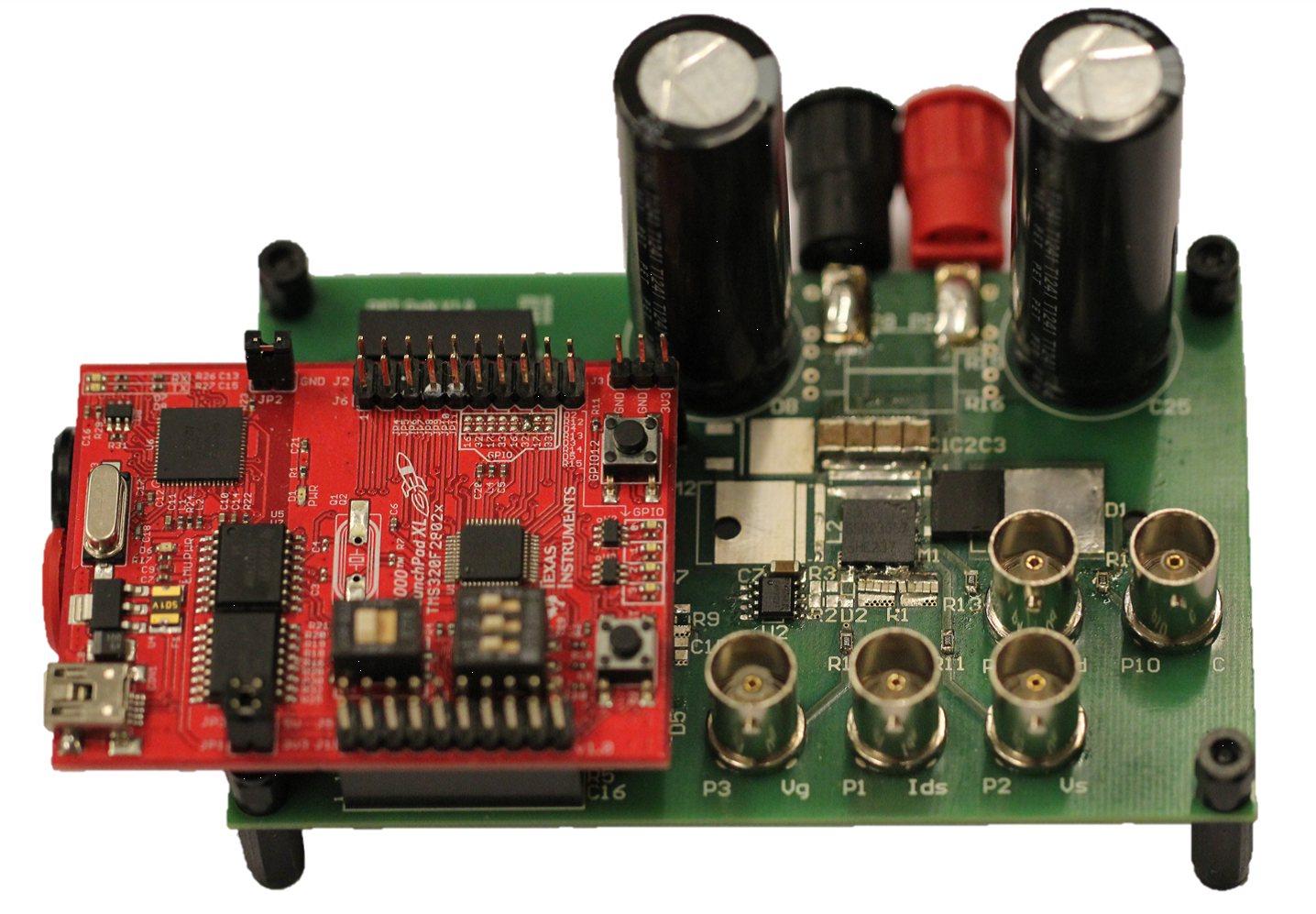
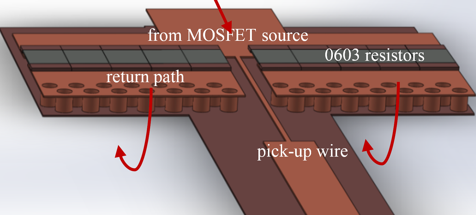
Figure 2: Measured vs. calculated PFC converter BCM switching frequency
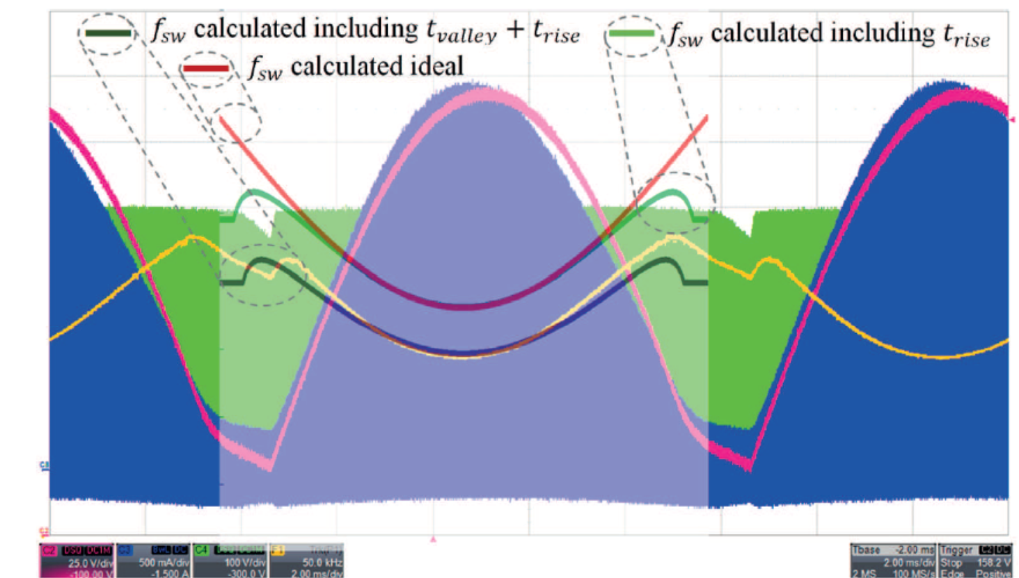
Figure 4: Implemented EQ20R inductors and conventional boost power stage
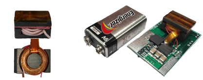
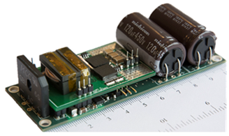
Figure 5: Integration of the proposed ZVS control and power stage PCBs
Contact Person

Zhe Zhang
Associate Professor
Technical University of Denmark
E-mail: zz@elektro.dtu.dk