The SiC inverter module is based on SiC BJT (Bipolar Junction Transistor) which requires a driver circuit, which can provide both high current and high voltage.
Driving a SiC BJT
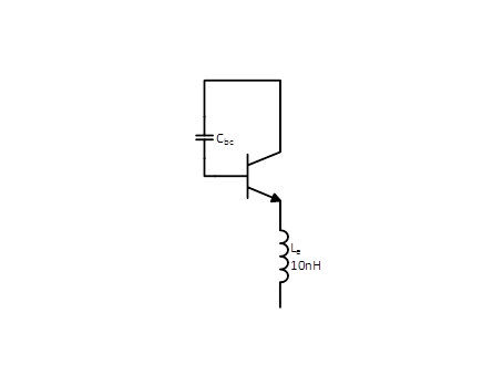
Figure 1. SiC BJT and the two most important parasitics for switching behavior
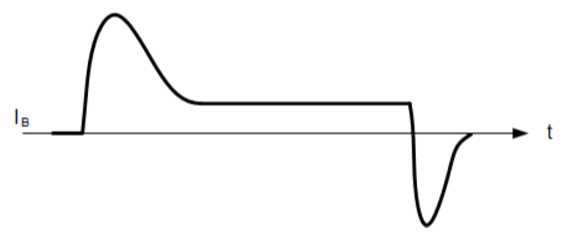
Figure 2. Ideal base current waveform
3 things to remember about driving a SiC BJT:
- Ensure that the transistor is always saturated when on
- During turn-on and turn-off, the base drive circuit must discharge and charge the Miller capacitance charge, QBC, quickly to reduce switching losses. That requires both high peak current availability and in practice high peak voltage availability too
- During turn-on and turn-off, the current in the parasitic emitter inductance needs to change. Change rate of current in an inductance is proportional to the voltage over the inductance. Therefore, the supply voltage to the driver affects the current switching speed
Power supply strategy for driver circuit
The developed driver circuit for the SiC BJT requires a high current low voltage supply for the base current during on-state of the SiC BJT. High voltage supplies, both negative and positive, are needed to switch the SiC BJT on and off very fast. Totally 6 floating supplies with 3 different output voltages are needed and they are generated from the DC-link voltage.
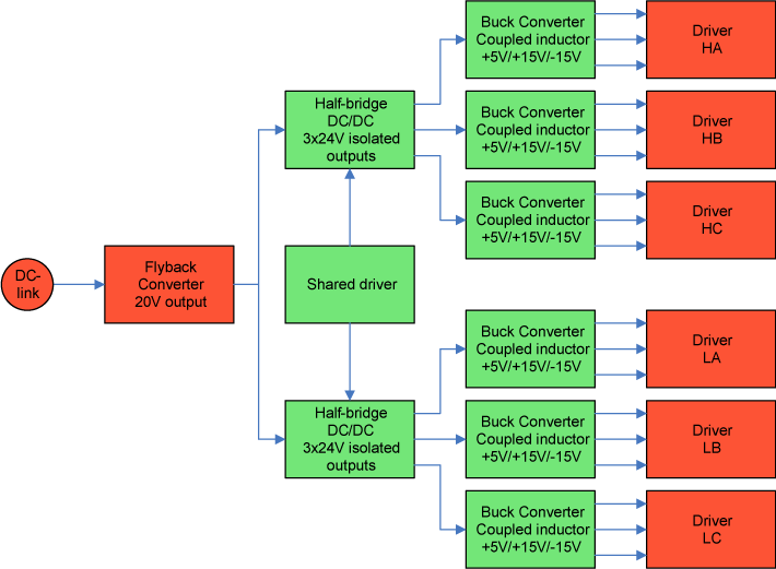
Figure 3. Block diagram of the power supply including driver circuits
(Red = located on inverter PCB, Green = located on PSU PCB)
Driver circuit
The driver circuit is located as close as possible to the pins of the inverter module in order to minimize stray inductance in the driver path. The power supply for the driver is located on a separate PCB.
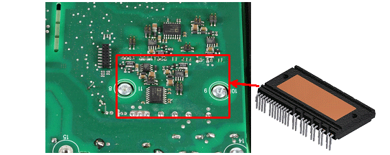
Figure 4. Driver circuit with local decoupling capacitors placed close to SiC inverter module
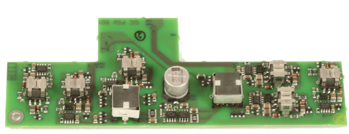
Figure 5. Power supply for driver on separate PCB
Results
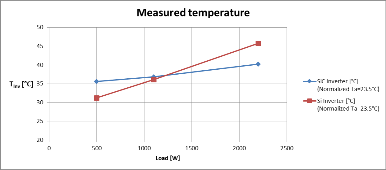
Figure 6. Measured heatsink temperature below inverter module
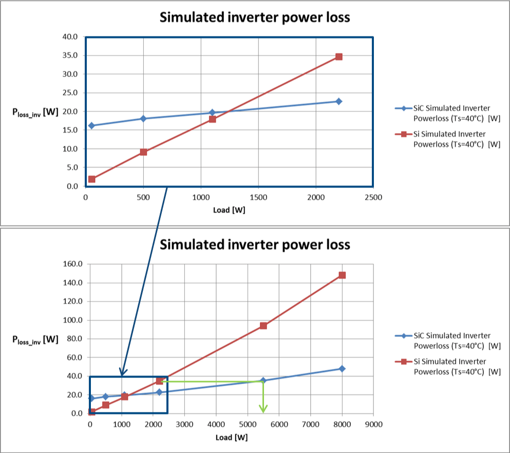
Figure 7. Simulated inverter power loss
Figure 6 shows the measured heatsink temperatures. Above 1200 W the SiC solution is colder than the Si solution.
In Figure 7 it is shown that also the simulated power loss is lower in the SiC solution above 1200 W.
The loss at low load for the SiC solution is higher than the Si solution. This is mainly because of the losses in the base drive due to the base current needed to drive the SiC BJT. At higher load the temperature is lower for the SiC solution.
The drive is designed for 2.2 kW but the potential is much bigger for the tested SiC inverter module at higher output power as the simulation shows. The Si inverter module dissipate 35W at 2.2kW load but the SiC inverter module reach 35W power loss at 5.5kW load which is an increase of 250% in output power.
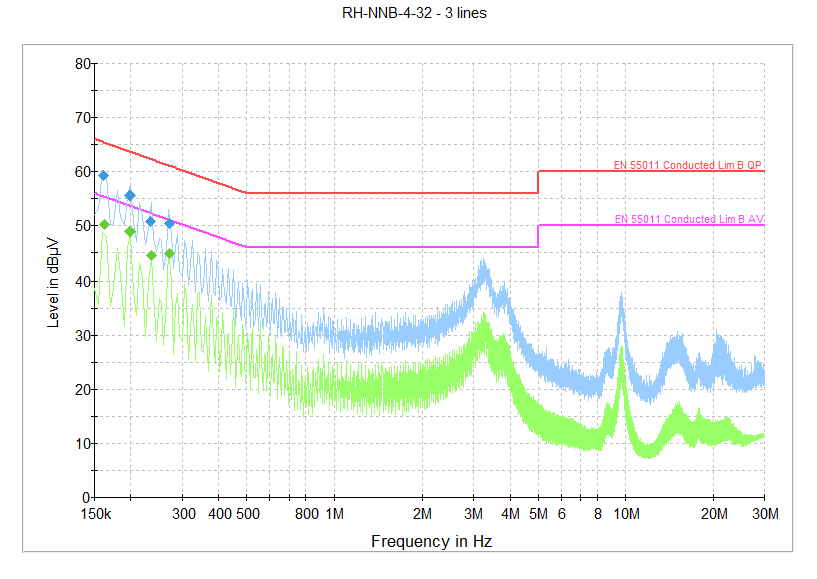
Figure 8. Conducted emission – Si-solution
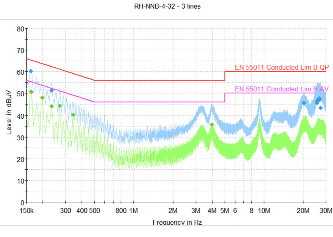
Figure 9. Conducted emission – SiC-solution
The EMI measurements shows increased conducted noise above 4 MHz for the SiC solution but still below the limits.
Contact Person
Søren Jørgensen
Development Engineer, Power Electronics
Grundfos Research & Technology
E-mail: soejoergensen@grundfos.com